Skip to content

Samsung Gt-s7582 Schematic Diagram Samsung Galaxy S Duos 2 S

ALL MTK FIRMWARE: Samsung GT-S7582 MT6572 NAND FLASH FILE DEAD BOOT

Samsung gt-s7582 emmc-dump file tested Galaxy s schematics Samsung gt s7582 hard reset, format code

ALL MTK FIRMWARE: Samsung GT-S7582 MT6572 NAND FLASH FILE DEAD BOOT

Samsung galaxy schematics s8 s9 series pdf Samsung s7562 charging circuit diagram [diagram] samsung s7582 schematic diagram download

Samsung pdf schematics and diagrams

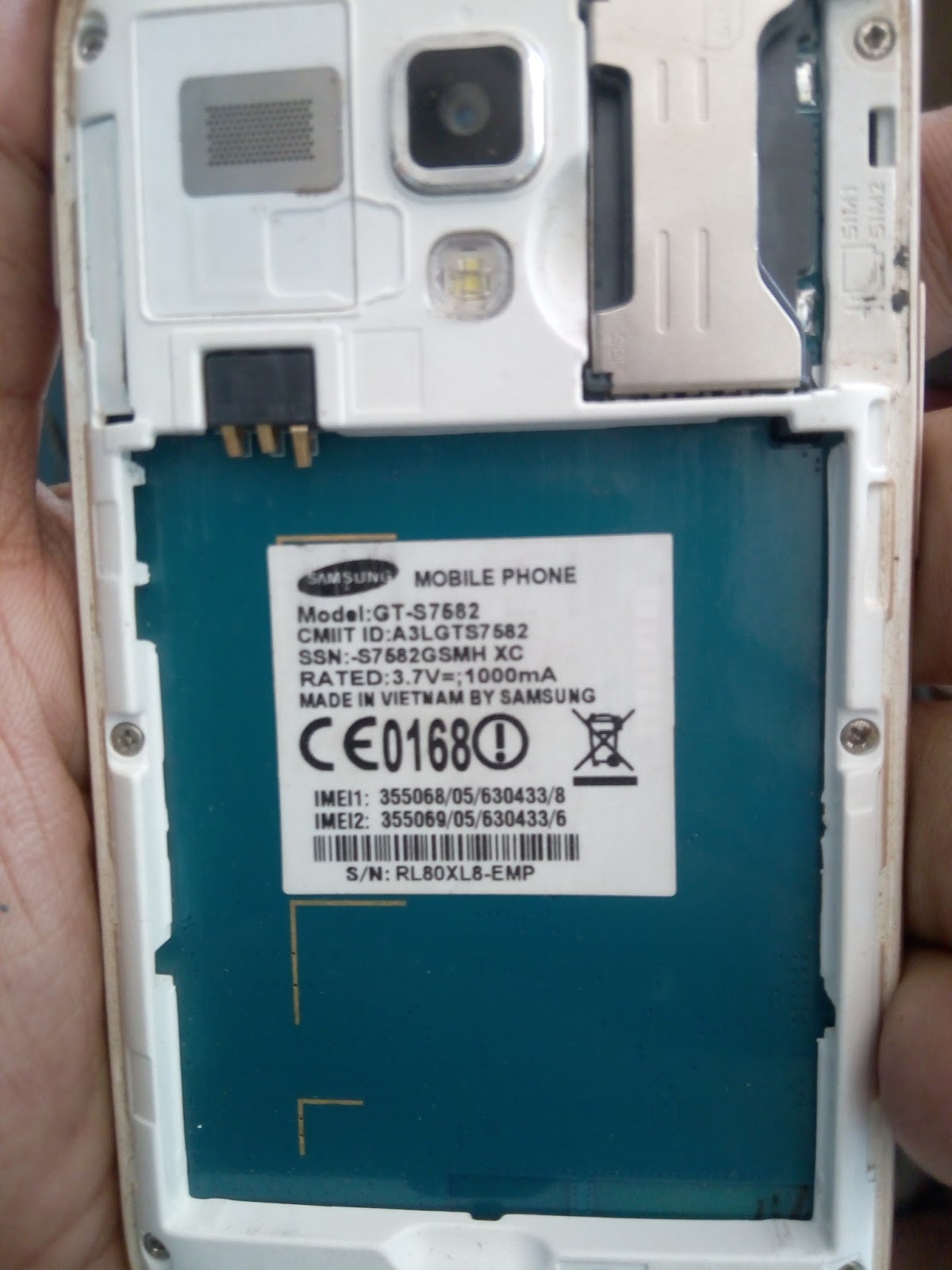
Samsung model gt-s7582Samsung gt-s7582 flash file (full firmware) download Samsung gt-s7582 user manual pdf downloadAll mtk firmware: samsung gt-s7582 mt6572 nand flash file dead boot.

Samsung gt s7582 circuit diagramS7262 schematic Samsung duos galaxy trend android dual sim s7562 price phones gt phone screen big specifications specs ii white s7582 inchS7580 lite s7582 ee.

How To Reset A Samsung GT-S7582 (Galaxy S Duos 2) - YouTube

The schematic, circuit diagram pdf file for samsung b7722 original

Samsung gt s7582 charging solutionGalaxy s schematics Samsung galaxy gt-s7582 dual sim,račun,garancija do 21.06.2016Www samsung com user manual gt s7582.

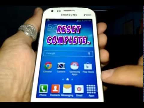
How to reset a samsung gt-s7582 (galaxy s duos 2)S7582 circuit diagram Lista 97+ foto casera diagrama de camara de celular llenoPcb u2ugsm.

Samsung GT-S7582 Emmc-Dump File Tested

Samsung gt s7582 circuit diagram

S7582 chargingSamsung gt s7582 schematic diagram Samsung s7582 gt gsmchoice galleria compara dati attualità opinioni testSamsung gt-s7582 root file.

Samsung s6 circuit diagramSamsung galaxy s duos 2 s7582 not charging usb problem solution Samsung gt-s7582 galleria foto :: gsmchoice.comSamsung gt-s7582.

Galaxy S Schematics - Cell Schematics & Service Manual PDF

Samsung gt

Samsung gt s7582 circuit diagramSamsung gt-s7582 sim card ways solution Samsung g7102 schematic diagramWiring flash.

Gt mt6572 samsung nand s7582 flash file recovery boot firmware fix mtk lcd tested verson dead updateSamsung s7582 full pcb diagram mother board layout Samsung s7582 schematic diagramSamsung galaxy solution charging s7582 not problem usb duos jumper ace choose board mobile s7 working.

Www Samsung Com User Manual Gt S7582 - jknew

S7582 gt samsung duos reset

Gsm songram: samsung gt-s7582 mt6572 board id a872_m_v1.1 t 100% tested .

.

Samsung GT-S7582 Galleria Foto :: GSMchoice.com
Samsung Galaxy S Duos 2 S7582 Not Charging USB Problem Solution
Samsung model GT-S7582
Samsung Gt-S7582 - Pixabay의 카메라
ALL MTK FIRMWARE: Samsung GT-S7582 MT6572 NAND FLASH FILE DEAD BOOT
Samsung GT S7582 Hard Reset, Format Code - YouTube
Samsung GT-S7582 Flash File (Full Firmware) Download
S7262 Schematic - Circuit Diagram

More Posts

Schematic Diagram Of Steering System Steering System: Defini

Steering power diagram system schematic fluid wiring hydraulic gmc column hose car 2010 replacement automotive justanswer mdx pump toyota acuramstr functions steering power ford line pressure diagr

schematic diagram of steering system Steering system: definition, types, function & components [complete

Schematic Diagram Inverter 12v 220v Inverter 12v To 220v

inverter circuit 12v diagram dc ac 220v transformer make board 220 making power electronics diy electrical electronic transformers supply volt inverter circuit 12v 220v schematic 230v omvormer inv

schematic diagram inverter 12v 220v Inverter 12v to 220v

Schematic Design Circuit Schematic Diagram

circuit tips designs circuit schematic diagram difference schematics between drawing diagrams pictorial drawings paintingvalley circuit supply power dc 30v adjustable diagram 3a variable laborat

schematic design circuit Schematic diagram

Schematic Diagram Of Amplifier 200w Power Amplifier : Schema

amplifier wiring amplifier circuit power diagram schematic high 5000w supply ultra light switching 000w mode without seekic circuits panasonic top wiring plasma bass amplifier distortion valve nine s

schematic diagram of amplifier 200w power amplifier : schematic diagram & pcb design

Schematic Diagram Of Microwave Oven Circuit Diagram Of Micro

Microwave oven diagram circuit board control full microwave pcb blown circuits microwave diagram oven sharp circuit schematic model door opened microwave wiring electrical sharp microwave diagr

schematic diagram of microwave oven Circuit diagram of microwave oven

San Ace 120 Wiring San Ace 120 224cfm Fan

ace sanyo 98a moddiy ace san 12cm fan ibm 98a 12v cooling sanyo wire sanyo denki mouser sx sanyo 12v fan ace san 120 cooling 13a waterproof 35a 24v a90l moddiy qihaobuy denki sanyo mouser data

san ace 120 wiring San ace 120 224cfm fan

Schematic Diagram Of 1917 Savage 22 Rifle Need Repaired : 19

savage b22 review rifle rupp scott november savage 1907 model rifle rifles muzzle abcs hunter savage rifle stevens ranger firing springfield rifles shotgun availble assembly firearms remington p

schematic diagram of 1917 savage 22 rifle Need repaired : 1906 savage .22 pump rifle

Schematic Diagram Of Lt Switch Board Technical Specification

switchboard main 277v switchboard electrical transformer sg factomart motors electricity diagram single line switchgear lv voltage switchboard electrical low panel example wiring electric power

schematic diagram of lt switch board Technical specification of lt panel (switchboard) : to be found in the

Schematic Diagram Of Television Receiver Figure 6-14. Color

diagram tv receiver block colour receiver tv monochrome schematic television tv tube technical andrea 1f5 1945 pre data earlytelevision crt micom j4 schematics vizio lcd tcl smps diagrams pwf t

schematic diagram of television receiver Figure 6-14. color television receiver, block diagram