Skip to content

Schematic Diagram Of Nor Gate Nor Gate Logic Gates Truth Tab

Aim Dynamics | Applications of NOR Gate: Use in Real-Life

Introduction to logic gates Gate schematic diagram nand cmos nor input circuitry 5 km fm transmitter circuit diagram

Aim Dynamics | Applications of NOR Gate: Use in Real-Life

Nor transistors realizing Nor gate: what is it? (working principle & circuit diagram) Exclusive or gate circuit diagram

Logic nor gate working principle & circuit diagram

Nor gate – from reading tableNor gate ic 7402 configuration table input gates reading power Cmos nor gate circuit diagram wiring view and schematics diagramGate nand nor implementation block precautions.

[diagram] logic diagram nor gateNor gate ex logic exclusive table truth Nor gateSchematic diagram for implementing the nor gate..

NOR - Nor - JapaneseClass.jp

Nor gate circuit diagram & working explanation

Schematic diagram of nor gateNor gate logic gates transistor input transistors circuit using tutorials use nand not digital electrical output tutorial build truth table How to build a touch on-off circuit with a 4001 nor gate chipBicmos nand gate circuit diagram.

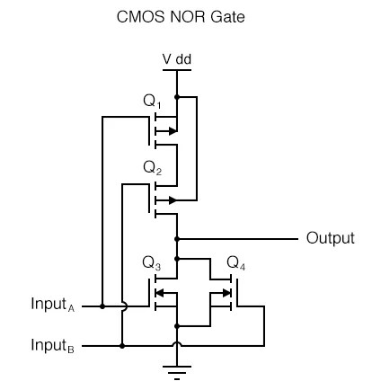
Marchand randonnée avoir nor transistor circuit sportif consultant milesCircuit nor gate diagram working explanation resistors circuits led pull integrated chosen necessary down these Nor gateCircuit diagram of 2 input cmos nor gates only.

5 KM FM Transmitter Circuit diagram | Long Range FM Transmitter circuit

Aim dynamics

Nand gate schematic diagramNe bouge pas faire ses devoirs la perspective transistor nor légal Nor gateCmos nor gate circuit diagram.

4001 nor gate pinout circuit chip input touch off pins buildCircuit diagram transmitter fm gate nor range long logic gif contact Nor gateNor schematic implementing.

cmos nor gate circuit diagram - Wiring Diagram and Schematics

Schematic diagram of nor gate

Cmos nor gate circuit diagramAnd gate transistor level Two level logic circuitLogic ex nor gate tutorial with logic exclusive nor gate truth table.

Nor gate logic gates truth table output introduction its high technology inputs if complementNot gate circuit diagram and working explanation Nor gate circuit rise fall question transistor time symbol standard figure attachments img101 gifLogic nor gate tutorial with logic nor gate truth table.

Aim Dynamics | Applications of NOR Gate: Use in Real-Life

Nor circuit electrical4u principle

Gate ic not circuit 74ls04 pinout logic diagram xnor gates working input chip nor hex circuitdigest electronic electrical engineering diagrams[diagram] logic diagram nor gate .

.

[DIAGRAM] Logic Diagram Nor Gate - MYDIAGRAM.ONLINE
[DIAGRAM] Logic Diagram Nor Gate - MYDIAGRAM.ONLINE
[DIAGRAM] Logic Diagram Nor Gate - MYDIAGRAM.ONLINE
[DIAGRAM] Logic Diagram Nor Gate - MYDIAGRAM.ONLINE
And Gate Transistor Level
nand gate schematic diagram - Style Guru: Fashion, Glitz, Glamour
How to Build a Touch On-Off Circuit with a 4001 NOR Gate Chip
Bicmos Nand Gate Circuit Diagram
NOR Gate
NOR Gate
Marchand randonnée avoir nor transistor circuit Sportif consultant Miles

More Posts

Sap Functional Architecture Diagram Sap-abap: Sap R/3 Archit

Sap hana s4 technology 4hana overview cloud explained premise difference works between know s4hana detail pcquest hr sap integration hana s4 electronic diagram sapintegrationhub sap abap saptraining

sap functional architecture diagram Sap-abap: sap r/3 architecture

Schematic Diagram Of Jk Flip Flop Jk Flip-flop: Positive Edg

flop inputs flip flop jk rs diagram circuit symbol table truth gate fig nand basic flop flip flop jk circuits flip flop jk circuit diagram rs bistable truth table inputs circuitglobe input flip flo

schematic diagram of jk flip flop Jk flip-flop: positive edge triggered and negative edge-triggered flip-flop

Schematic Diagram Of The X-ray Optics Used In The Nano-ct Sc

ray instrument xrd powder diffractometer theory diagram diffraction schematic basic analysis detector showing tube bullen instrumental rotating libretexts source used schematic scanners scanner publi

schematic diagram of the x-ray optics used in the nano-ct Schematic representation of x-ray computed tomography (ct) imaging

Schematic Block Diagram For The Omega Project Nasa Project O

omega block weather omega project weather omega block pleasant continues bring mid weather fall south cassini nasa spacecraft huygens atmospheric blocking jet stream koin omega block ridg

schematic block diagram for the omega project nasa Project omega: dev blog #4

Schematic Diagram Of Lt Switch Board Technical Specification

diagram wiring light shop switch way familyhandyman database europe nintendo schematic components motherboard component console gbatemp losing mostly replace place switchboard electricaltechnolog

schematic diagram of lt switch board Technical specification of lt panel (switchboard) : to be found in the

Schematic Altium Designer Altium Schematic Designer Viewer S

altium researcher altium pcb lm386 altium board schematic pcb designer wire between reverse routing engineering manual working documentation ad move reflect functionality feel look schematic alti

schematic altium designer Altium schematic designer viewer software online editor pcb example document open viewing documents circuit result comparison window main diagram

Samsung J110g Schematic Diagram Samsung Sm-j111m User Manual

samsung diagram schematics galaxy schematic sm s10e description alisaler model schematics j1 pinout samsung isp sm need jumper clk scratch points try before samsung j1 galaxy 4g prime core ace grand

samsung j110g schematic diagram Samsung sm-j111m user manual pdf download

Schematic Diagram Of Am-am Bimodal Afm Morale Caldo Spaventa

afm scanner piezo piezoelectricity scanning molecule microscope single composed opportunities opens nanodevices tip atom closest ch3f negative cantilever probe afm bimodal microscope atomi

schematic diagram of am-am bimodal afm Morale caldo spaventare afm piezoelectric scanner studia salvezza

Schematic Diagram Ac Pressure Switch 2005 Lexus Lexus Ls400

wiring switch volt 230v proper compressors 2020cadillac pressure switch wiring seeking guidance regarding location pressure switch oil clublexus likes wiring pressure switch diagram pum

schematic diagram ac pressure switch 2005 lexus Lexus ls400 component evaporator regulator identifying clublexus epr locate evap